Digital devices, such as computers, operate by using binary logic. That is, the wires that interconnect components, both on integrated circuit chips and between chips at the circuit board level, take on only two voltage levels of significance - which are labelled 0 and 1. Typically, a voltage near 0 Volts is used to represent a binary 0 and a voltage near 5V to represent a binary 11.
Binary numbers
As children, we learned to count using our 10 fingers (aka digits). Hence we utilize the arabic numerals for which there are 10 digits 0, 1, 2, 3, 4, 5, 6, 7, 8 and 9. Temporarily ignoring the convention of omitting leading zeros, we’re all familiar with the pattern of repeating sequences of digits in each column, whereby each cycle of a lesser significant column causes an increment of the next significant column.
000
001
002
003
004
005
006
007
008
009
010
011
012
013
014
015
.
.
.
098
099
100
101
.
.
This familiar numbering system is known as Base 10 arithmetic, or Decimal. By analogy, if we restrict ourselves to using only 2 digits (0 and 1), then we have Base 2 arithmetic - Binary. Counting in binary follows the same pattern of repeating all digits in a lower significance ‘bit’ before incrementing the next column, and then cycling back to the first digit (0):
000
001
010
011
100
101
.
.
Don’t be confused by the fact that we’re re-using 0 and 1 from the arabic digits, we could have just as easily invented new symbols or used A and B etc. However, using 0 and 1 is the convention and unfortunately that means that a binary number like 011 looks very similar to the decimal number 11 even though they have different values. Where there is any confusion, we’ll write a trailing “b” to indicate binary and omit leading zeros from decimal numbers. Here is the numeric equivalence between some binary and decimal values:
000b = 0
001b = 1
010b = 2
011b = 3
100b = 4
101b = 5
110b = 6
111b = 7
Each column in a binary number is referred to as a Bit. Hence, numbers can be represented in digital circuits by a set of wires taking ~0V to represent a 0 and ~5V to represent a 1. So, using 3 wires, we can represent any number between 0 and 7 by using the appropriate combination of voltages to represent the binary values between 000b and 111b.
Binary addition
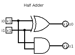
Suppose we want to create a digital circuit for adding two bits. The output will also need to be two bits. If we label the two input wires/bits i0 and i1 and the output bits s0 and s1 (s for sum), then we can write down a table indicating what we wish the circuit output to be for each possible combination of the two input bits:
i1 i0  s1 s0
0  0   0  0
0  1   0  1
1  0   0  1
1  1   1  0
Notice that each input can only represent the number 0 or 1, where as if we group the two output wires as a single 2-bit number, it can represent 00b through 11b (i.e. 0 through 3). Now, the circuit only needs to compute any of 0 + 0 = 0, 0 + 1 = 1, 1 + 0 = 1 and 1 + 1 = 2 - that is (in binary) 0b + 0b = 00b, 0b + 1b = 01b, 1b + 0b = 01b and 1b + 1b = 10b.
This is a primitive building block for circuits that can perform arithmetic on larger binary numbers, such as addition, subtraction, multiplication and division. The circuit that can implement it is known as a Half-Adder. This will be the first circuit we construct using the digital simulation tool. However, before we can do that we need to introduce an even more primitive digital component: the Digital Logic Gate.
Logic Gates
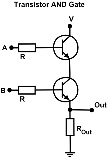
Ultimately, a silicon chip is constructed from analog electronic components, such as transistors and resistors. However, as digital designers, we prefer to work at a higher-level of abstraction - the digital logic gate.
Below are the circuit symbols for 8 common logic gates2, but we’ll first concern ourselves with the primary three from which the others derive: the AND, OR and NOT (inverter) gates.
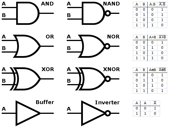
The function of each gate is described using a table of 0s and 1s - which is known as a Truth Table (on account of the association of 0 with false and 1 with true in Boolean logic). Notice also, that the column headings use a notation whereby OR is written using the + sign and AND is written with a dot. This is analogous to multiplication and addition in mathematics, but again is just a borrowing of symbols. We’ll typically explicitly use AND, OR and NOT, though you’ll see this mathematical notation in other contexts. The NOT, or inverse, is indicated by a line over the input name, or sometimes in other contexts a prime/dash.
So, that do the gates do? In words, the inverter, or NOT gate, has one input and one output. When the input is 1, the output is 0 and vice-versa. The AND and OR gates both have two inputs and one output each. The AND gate’s output is a 1 only if both the inputs are 1 (i.e. the A AND the B input are 1 => the output is 1). Similarly, the OR gate’s output is 1 if either the A input OR the B input is a 1.
The other gates are just variations: the NAND gate (NOT AND) is like the AND gate, but its output is inverted (the opposite of the AND for the same inputs). Similarly, the NOR (NOT OR) is an inverted OR gate. The XOR gate (eXclusive OR) is like OR except for the case when both inputs are 1, when it has a 0 output instead. The buffer is essentially the identity gate and it isn’t typically used explicitly in digital design (though in practice it might be used to boost the voltage to ensure a 1 doesn’t become a 0 due to flagging voltage dropping closer to 0V).
Interestingly, every circuit created using any of the 8 gates above, no matter how complex, can be reduced to one using only NAND and NOR gates alone. On silicon chips, the gates are implemented directly using analogue components (which vary by chip technology).
Using Logisim
Logisim is a Java-based application written by Carl Burch. It can be downloaded from his Logisim website. Being Java-based, it will run on most platforms by using the .jar file directly. For example, from a terminal shell, just enter java -jar logisim.jar (substituting the exact filename). There is a Windows specific download. The Mac specific download will prompt for installation of an older version of Java, so best to run it directly from the .jar file.
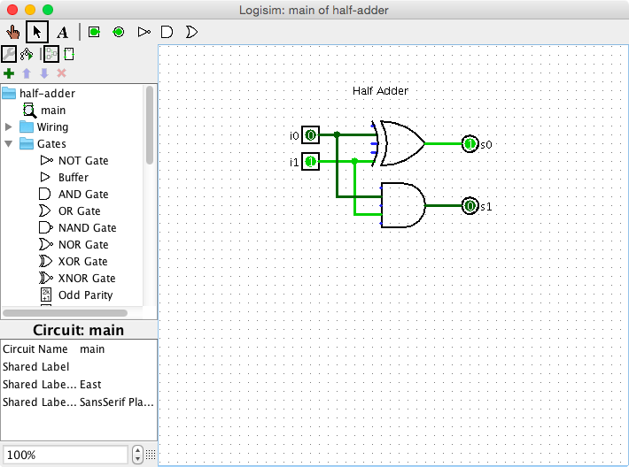
Once you have Logisim open, you can experiment with the gates we’ve just learned about. Use the green pin icons in the top toolbar to place inputs and outputs. Using the hand icon you can ‘poke’ the inputs to toggle their value between 0 and 1. Just single-click to select a gate from the left panel, then place it on the sheet. Connecting the pins via wires is just a matter of clicking and dragging. A more detail explanation of how to use Logisim is available via its documentation.
Note: the gates in Logisim can have more than two inputs, in which case they behave as a cascade of the primary two-input gates. We’ll not use this functionality directly as the actual gates available in FGPA hardware take the standard two inputs.
Multiple bit binary addition
Having a circuit that can add 1+1 at most isn’t terribly impressive. Let us see how to extend that to multiple bits representing larger numbers.
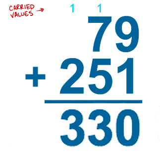
Recall how you learned to do decimal addition of large numbers in school. If the sum of digits in a given column was greater than 9 (the last available decimal digit), then you had to carry one into the next column (which represents values 10 times larger).
Notice also, that any decimal number can be re-written as a sum of coefficients multiplied by powers of 10 (using * for multiplication):
Now, adding in binary is exactly analogous - except we have to carry 1 when the sum for one bit is greater than 1 (the last available binary digit). Each more significant column to the right represents values 2 times larger. The easiest way to convert between decimal and binary representations is to use you calculator. Most professional calculators and likely the calculator app on your desktop, have a scientific or programmer mode which supports binary. My calculator tells me that 79 = 01001111b and 251 = 11111011b
Just as a decimal number can be written as a sum of powers of 10, so a binary number can be written as a sum of powers of 2.
 79 = 01001111b = 0*27 + 1*26 + 0*25 + 0*24 + 1*23 + 1*22 + 1*21 + 1*20
251 = 11111011b = 1*27 + 1*26 + 1*25 + 1*24 + 1*23 + 0*22 + 1*21 + 1*20
Now we can add:
C   11111111
A   001001111
B  +011111011
   ----------
S   101001010
The top row are the 1s that were carried. We had to expand the number of bits we’re adding to 9 to accommodate the answer as it is greater than 28 = 256. For example, to start, add 1b + 1b = 10b, which implies placing the 0 in the first(rightmost/least-significant) column and carrying the 1. Next, we had to add 1b + 1b + 1b = 11b on account of needing to also add the carried 1. Hence, we placed 1 in the second column and carried again, and so on.
Our final answer was:
101001010b = 1*28 + 0*27 + 1*26 + 0*25 + 0*24 + 1*23 + 0*22 + 1*21 + 0*20 = 330
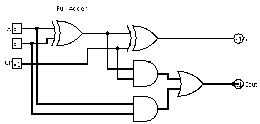
Note that for each column we needed to add 3 bits, on account of the carry bit, not just two. Hence, in order to build a circuit that can perform multiple-bit addition, we’ll need a 3 bit adder as a component for each column, with inputs for the bits from A, B and Carry. This is known as a Full Adder.
Full-Adder
Below is the truth table for the Full Adder circuit along with the corresponding decimal sum. We’ve renamed the inputs and outputs to conform to the convention for adders, where Cin and Cout indicate carry in and carry out respectively.
Cin A   B    Cout S      Decimal addition
0   0   0    0    0      0 + 0 + 0 = 0
0   0   1    0    1      0 + 0 + 0 = 1
0   1   0    0    1      0 + 1 + 0 = 1
0   1   1    1    0      0 + 1 + 1 = 2  (0 & carry 1)
1   0   0    0    1      1 + 0 + 0 = 1
1   0   1    1    0      1 + 0 + 1 = 2  (0 & carry 1)
1   1   0    1    0      1 + 1 + 0 = 2  (0 & carry 1)
1   1   1    1    1      1 + 1 + 1 = 3  (1 & carry 1)
We can satisfy ourselves that we’ve covered all possibilities for the 3 input bits, since we have 23 = 8 rows/combinations. Below is a standard circuit for a Full Adder. Go ahead and implement it in Logisim.
Boolean expressions
Boolean algebra was introduced by George Boole in 1847. This is essentially what we’re now referring to as digital logic. Hence, in addition to describing the behaviour of a logic circuit using either a truth table or a circuit diagram, as seen above for the Half and Full Adders, we can also write it using an algebraic notation, as follows:
Half Adder             Full Adder
s0 = i0 XOR i1         S = (A XOR B) XOR Cin
s1 = i0 AND i1         Cout = (A AND B) OR (Cin AND (A XOR B))
Notice that the two equations for the Full Adder share a common subexpression: A XOR B. The circuit implementation doesn’t duplicate the XOR gate to compute that intermediate result. It is worth noting that it is often possible to simplify logic expressions to minimize the number of gates used. Just as there are standard equalities in high-school algebra for simplifying algebraic expressions, so there are known equivalences in boolean logic that can be used to transform and simplify expressions. Typically, a digital designer would use software tools to automatically minimize the number and/or types of gates needed to implement a given logic circuit. We’ll using such a tool later on.
For example, a better way to express the Full Adder algebraically using one less XOR gate would be:
Full Adder
Sp = A XOR B
S = Sp XOR Cin
Cout = (A AND B) OR (CIn AND Sp)
Combining Full Adders to add 8bit numbers
We can combine 8 Full Adder circuits together to form an adder that can sum two 8 bit binary numbers. The corresponding bits of the 8bit inputs (we’ll also call A and B) each feed a single Full Adder and the Carry output from each ‘column’ Full Adder is wired to the Carry input of Full Adder for the next most significant bit/column. We also have an overall Carry input and output (in case we wanted to later utilize this 8 bit adder as a subcircuit for adding even wider bit widths).
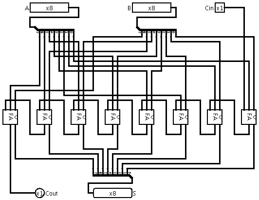
Some examples of adding 8bit values (useful for testing the 8bit adder circuit you’ll construct):
A           B           Cin  =  Cout  S              Decimal
00000000b + 00000000b + 0b   =  0b    00000000b      0   + 0   + 0 = 0   (0 carry 0)
00000011b + 00000011b + 1b   =  0b    00000111b      3   + 3   + 1 = 7   (7 carry 0)
11111111b + 00000000b + 1b   =  1b    00000000b      255 + 0   + 1 = 256 (0 carry 1)
10000000b + 10000000b + 0b   =  1b    00000000b      128 + 128 + 0 = 256 (0 carry 1)
10001111b + 00111111b + 0b   =  0b    11001110b      143 + 63  + 0 = 206 (206 carry 0)
11111111b + 11111111b + 0b   =  1b    11111110b      255 + 255 + 0 = 510 (254 carry 1)
11111111b + 11111111b + 1b   =  1b    11111111b      255 + 255 + 1 = 511 (255 carry 1)
The right-most bit is the least significant and is conventionally labeled bit 0, so our 8bit A and B inputs have bits 7-0 from left to right. The Carry output can be considered a 9th bit of the output (bit number 8 after bits 7-0 of S and consequently represents the decimal value 28 = 256).
Before we can create this using Logisim, we’ll need to learn how to use Logisim’s sub-circuit and multi-bit/bus wire features. Every project file within Logisim can actually have multiple circuit worksheets. New circuits can be added using the Project->Add Circuit menu option. Double-clicking switches the edit panel between the circuits, but just single-clicking to select a circuit allows to you use it as a component just as you have with other built-in components like gates. You can nest circuits within other circuits as deeply as needed.
By default, there is a single circuit named “main”, but you can edit the circuit name from the bottom-left Tool pane. Open the Full Adder circuit you created and change the name from “main” to “full-adder”. Optionally, you can use the Project->Edit Project Appearance menu option to switch from editing the circuit to editing how the circuit will appear when used as a sub-circuit component. For example, you can use the text tool to add the text “FA” on top of the circuit chip symbol, so that when used in other circuits it will be clear that it is a Full Adder at a glance.
Now, create a new circuit using the Project->Add Circuit menu selection and edit the name of the new (blank) circuit to be “8bit adder”. We’re going to need an 8-bit A input, an 8-bit B input, a 1bit Carry in then an 8bit S (sum) output and a 1bit Carry out. For the 8bit A input, we could use 8 separate 1bit input pins as we’ve used before, but Logisim supports drawing single wire lines that actually represent bundles of wires. Such bundle of parallel wires is commonly named a ‘bus’.
The bit-width of a wire in Logisim is determined by the bit-width of the component pins to which it is connected (which must be the same at both ends, or the wire will be rendered in orange and won’t function). Go ahead and place a pin on the circuit worksheet. Select it and notice one of the options in the Tool panel in the lower-left is “Data bits”. Edit this value to be 8bits (from the default 1bit). Now, the pin will show a row of 8 0s, which can be toggled using the ‘hand’/poke tool. Any wire connected to this 8bit wide input pin header, will be an 8bit bus wire - representing a bundle of 8 parallel wires (though still drawn as a single wire). You can label the pin using the text tool by clicking on it and entering “A”.
Now, while we could connect the 8bits directly to another 8bit wide pin, we actually want to break-out, or split, the 8 bits into individual 1bit wires in order to connect them separately to the 1bit A inputs of 8 Full Adders. To do this, we need what Logisim calls a “splitter”. Locate the splitter from the Wires subcategory and place it on the sheet (You’ll want to move it and rotate it into a similar position to that shown above. To rotate a component, select it and edit the “Facing” property in the bottom-left Tool pane).
Now, you can connect the 8bit A input to the single 8bit bus pin on the splitter and then you’ll be free to connect the 8 1bit ‘split’ pins individually.
Continue the construction of the 8bit adder circuit by placing 8 Full Adder circuits on the worksheet and then connecting them up as shown above (the A 7-0 bits to the corresponding A inputs of each Full Adder, same with B inputs, connect the Carry ‘out’s to ‘in’s in a cascade and connect all the S sum outputs from the Full Adders to the S 8bit output via another splitter). Notice that there is a ‘zoom’ control in the bottom-left of the Logisim window - which can be helpful for accurately connecting wires to pins that are close together. You can test the adder by manually entering different input bit sequences using the hand/poke tool.
When you’re first learning to use Logisim, you may need to adjust the positions and/or orientations of components and sometimes delete and re-connect wires to get everything connected correctly. Don’t forget to save your circuit.
Refer to the Logisim documentation for more details on how to use Logisim.
If you were successful, congratulations! - you’ve just created your first digital adder circuit (at least in software simulation).
Before we’re ready to implement an Artificial Neural Network using digital logic circuits, we’ll need to learn how to build fixed-point arithmetic and multiplication circuits. To understand why we need fixed-point addition and multiplication, we’ll first look at the basics of Artificial Neural Networks in the next section.
-
This is the so-called TTL (Transistor Transistor Logic) standard, though the internals of silicon chips may use other Voltages, for example in the 2-3V range. ↩
-
How do computers do math?, Coert Vonk, Accessed 2015-06-21. ↩